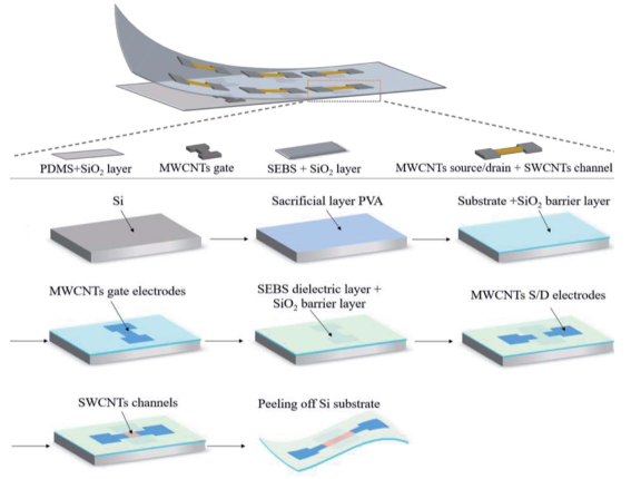
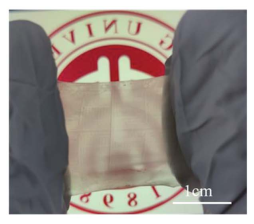
近期,本课题组张敏老师和焦浩轩同学分别以通讯作者和第一作者在RSC ADVANCES上发表了题为“Intrinsically stretchable all-carbon-nanotube transistors with styrene–ethylene–butylene–styrene as gate dielectrics integrated by photolithography-based process”的研究成果。
In this work, we have introduced a plasma resistant layer to protect the polymer dielectrics and elastomer substrate from plasma etching or long-term UV light. Based on that, we have realized integratable stretchable all-carbon-nanotube thin film transistors by the traditional lithography–etching-based process platform. In this design, we adopt an organic material, styrene–ethylene–butylene–styrene (SEBS), as gate dielectric considering its lower viscosity and hysteresis performance. And we use carbon nanotubes (CNTs) as channel and electrode materials in the all-carbon-nanotube transistors.
In conclusion, we have realized intrinsically stretchable transistors by traditional photolithography and O2 plasma etching based process. These transistors have small channel length of 20 μm and channel width of 56 μm, which is a prominent size for stretchable transistors. These transistors show a high carrier mobility of 10.45 cm2V-1s-1, with Ion/Ioff over 103 on its initial state. Even after they are stretched by 50% tension for 500 times, they can still maintain relatively good electrical characteristics, with the mobility kept at 2.01 cm2V-1s-1 and the Ion/Ioff kept at 103. This work provides a good solution to achieve high mobility, miniaturization and integration of stretchable transistors. Hopefully, this integration method based on the traditional process platform can play an important role in shaping the future of stretchable electronics.
文章链接:
https://pubs.rsc.org/en/content/articlelanding/2020/RA/C9RA10534D

