4.1 Design of power management system on display driver IC
 |
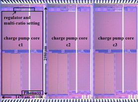 |
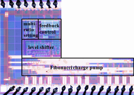
Traditional power management system includes low-dropout regulator(LDO), Charged DC-DC converter and charge pump. As the power supply of display driving IC, it may be more than 30 V (global power supply is 2.4 V ~ 3.6 V), which means high voltage conversion ratio is required. Because the supply current of display driving IC is medium (< 10 mA), we choose Dickson, Fibonacci, series parallel, voltage doubler and other charge pump types. In this project, we propose six novel charge pump topologies, three of which have successfully completed the flow sheet, and the test results are good. Due to its good compatibility, it is proposed to be applied to a large number of related products. The three structures are as follows: 1. Fibonacci CPS charge pump IP with strong driving ability and high power efficiency; 2. High integrated and efficient DIC FIB charge pump IP; 3. FIB DIC FIB charge pump IP with a compromise between integration and driving current. At the same time, we propose a high-precision and simple algorithm model for charge pump topology analysis. These algorithms are expected to be used to promote the computer-aided design process of power chip in the future.
4.2 AMOLED Peripheral compensation circuit
AMOLED is considered to be one of the next generation display technologies, with the advantages of wide chromaticity, high resolution, lighter and thinner, but there are still problems of life and yield. Generally speaking, there are two kinds of TFT tubes used in amoeld pixel circuits, LTPS and a-Si (now generally IGZO). The mobility of LTPS TFT is good, it can provide N-type transistor and p-type transistor, but its uniformity is not good. The mobility and threshold voltage of LTPS TFT at different positions on the panel are not consistent; The uniformity of a-Si TFT is better, but its mobility is very low and it can only provide N-type transistors. In addition, with the aging of devices, the mobility and threshold voltage of a-Si TFT will drift continuously, resulting in poor display effect.
Many different pixel circuits have been proposed to solve these problems. However, due to the small number of internal tubes in the pixel circuit and the high requirements on the area, it is difficult to realize the internal compensation for the mobility and threshold voltage of OLED and driving TFT tubes perfectly. Therefore, the project team proposed a peripheral compensation circuit to compensate for aging and drift.
4.3 Design of high precision distributed low-dropout regulator for AMOLED display driver chip
 |
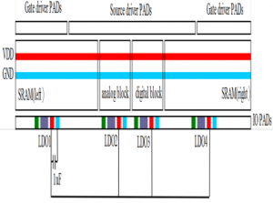 |
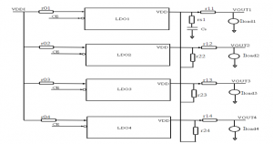
This project proposes a power management system architecture of AMOLED display driver chip, and analyzes and designs the sub module circuit of the system. Based on the global foundry 0.18um process, cadence software is used to debug and simulate the design circuit, and finally the power management system that meets the requirements is obtained. The driver chip designed in this project can drive the AMOLED display panel with 1920rgbx1080dot pixels, and the chip size is 20mmx3mm. According to the characteristics of the chip and its demand for power supply, the distributed voltage regulation scheme is adopted. Four LDOS are used to supply power to two SRAM, analog module and digital module on the drive chip, which reduces the load regulation rate of LDO and ensures the accuracy of the supply voltage of each module. At the same time, the external capacitance of 1uF is used for frequency compensation to ensure the stability of LDO.